Home
Projects
Articles
Support
☰
Home
Projects
Articles
Support
☰
Milling PCBs in-house enables rapid prototyping of new designs. Below are insights gained from utilizing a CNC machine for the creation of double-sided PCBs.
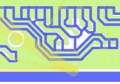
FlatCam is the preferred tool for converting Gerber files to gcode. Manual placement of cutting paths on the boards has proven more effective than relying on automatic isolation routing. While this method is more time-consuming, it allows for optimization of tool paths and the selection of different tools for specific areas. The result is a significantly smaller gcode file, faster processing times, and reduced tool wear.
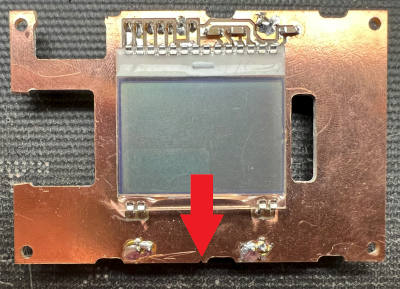
Achieving accurate alignment when flipping the board is a common challenge. One effective approach involves placing a via along the bottom edge of the PCB at the precise X-axis center and shifting the imported Gerber file in FlatCam so that this via aligns with the coordinates (0,0). Mirroring the board across the Y-axis at the point (0,0) before generating the tool paths for the underside ensures that, after flipping the board, the via can be used to re-align the work origin at (0,0). This method ensures that the mirrored paths align properly, provided the X-axis is not angled.
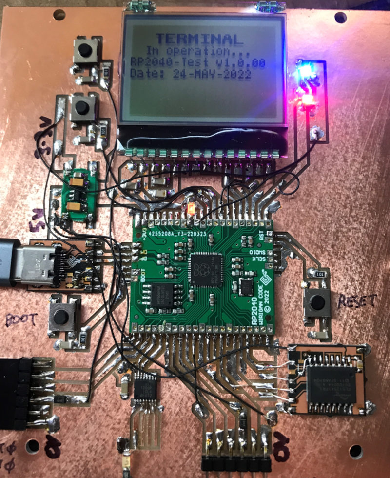
For holes requiring electrical continuity between the top and bottom layers, 33AWG wire can be used. Given that most header pins or connectors are soldered from the bottom of the board, if continuity to the top side is needed, the wire should be inserted and soldered into the hole before fitting the connector. Alternatively, the board layout can be designed to avoid the need for header pins to be electrically continuous with the top side. It is crucial to allow extra copper space around the holes to compensate for potential alignment errors when the board is flipped. A 70mil diameter pad with a 31mil hole is typically used at vias to accommodate a 1/32 inch tool diameter. Misalignment of up to 10mils is common.
Attention should always be given to ensuring extra copper space around the holes to account for alignment errors when the board is flipped. We generally use 70mil diameter pad and a 31mil hole at vias to suit 1/32 inch tool diameter. A mis-alignment of up to 10mils is typical.

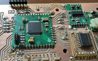
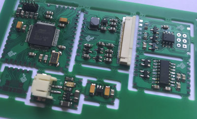
Producing sub-circuits simplifies the addition of complex and small components to a CNC-milled prototype. This also facilitates the desoldering and reuse of parts across different design iterations.
Milling PCBs presents several challenges: